
Inside China’s Advanced Packaging Rush
AI Is Pushing China’s Packaging and Testing Industry into System-Level Computing Competition

Advanced packaging is no longer merely an “upgrade of back-end processes.” In the AI era, it has become a strategic channel for reorganizing chips, memory, substrates, materials, equipment, and system performance.
This essay is part of China Industry Signals.
Executive Summary
China’s advanced packaging industry is moving from traditional OSAT capacity toward AI-era system integration, where 2.5D/3D packaging, Chiplet, HBM-related packaging, wafer-level packaging, fan-out, TSV, hybrid bonding, and glass substrates are becoming strategic technologies.
Chinese companies such as JCET, Tongfu Microelectronics, Huatian Technology, SJ Semiconductor, Forehope, and other domestic packaging players are expanding from conventional assembly and testing into higher-value advanced packaging platforms.
The strongest industrial signal is that advanced packaging is being pulled by AI computing, domestic GPU demand, HBM constraints, Chiplet architecture, and the global shortage of CoWoS-like capacity.
China’s path is not a simple copy of TSMC’s CoWoS model. Domestic players are moving through multiple routes: 2.5D/3D integration, wafer-level packaging, fan-out, SiP, TGV glass substrates, advanced packaging equipment, and packaging materials.
Packaging materials and equipment are becoming as important as packaging houses themselves. CMP, temporary bonding, electroplating, underfill, molding compounds, photo-sensitive PI, thermal interface materials, and glass substrates are all entering the advanced-packaging bottleneck map.
China still faces gaps in high-end customers, yield control, HBM integration, interposer capacity, advanced substrate supply, thermal management, and global ecosystem depth, but advanced packaging is becoming one of the most realistic channels for China to improve system-level semiconductor capability.

Lotus (荷花), by Lin Fengmian (林风眠), 1977
Its luminous white blossoms rising from dark water mirror the core argument of this essay.
Before an AI accelerator is actually installed inside a server, it must first pass through a place that is becoming more crowded, more expensive, and more decisive: the packaging line. The GPU, ASIC, I/O chips, and memory chips produced by fabs are not yet systems capable of releasing computing power. They must be diced, tested, redistributed, connected, and stacked, then organized together with HBM, substrates, thermal structures, and power-delivery networks into a high-performance package that can operate stably. This process used to be discussed as “back end.” In the AI era, it has moved to the front stage of whether computing power can actually be delivered.
The most interesting thing about advanced packaging is that it does not look as spectacular as lithography, yet it is increasingly determining the most practical delivery bottleneck in the AI chip supply chain. Designing a more powerful GPU is one thing. Stably connecting that GPU with multiple HBM stacks and making it run over the long term under high power, high bandwidth, and high thermal density is another. The reason CoWoS capacity tightness affects the global AI supply chain is precisely that advanced packaging is no longer just about “sealing chips.” It is about reorganizing chips, memory, interconnects, materials, thermal management, and system performance.
Chinese companies are entering the part of the industry where this shift is most intense. JCET, Tongfu Microelectronics, Huatian Technology, and SJ Semiconductor used to be understood mainly as part of OSAT capacity and traditional packaging capability. Now they are being viewed through the lens of 2.5D/3D packaging, Chiplet, wafer-level packaging, high-performance computing, domestic GPUs, and HBM-related processes. At the same time, equipment and materials companies such as Hwatsing, ACM Research Shanghai, Dinglong, PhiChem, Hysol Huawei Electronics, and WG Tech are also being pulled into the same industrial map by advanced-packaging demand.
This is what makes China’s advanced packaging industry worth watching. It is not a single company’s expansion story, nor is it a simple copy of TSMC’s CoWoS model. It is more like a reorganization of system capability: packaging houses, memory companies, AI chip designers, equipment companies, materials companies, substrate suppliers, and glass-processing firms are all repositioning around the real problem of AI computing delivery. Advanced packaging is pushing China’s semiconductor industry from single-chip competition into more complex system-level computing competition.
1. Packaging Is Moving from a Back-End Process into Computing Infrastructure
For a long time, packaging and testing were often viewed as the “back end” of the semiconductor value chain. After wafer fabrication, chips were diced, packaged, tested, and delivered to customers. This link was certainly important, but in the traditional narrative, it did not occupy the center of attention the way lithography machines, advanced process nodes, or GPU architecture did.
AI has changed all of this.
Training and inference for large models require increasingly higher computing density, memory bandwidth, interconnect efficiency, and energy-efficiency control. The transistor count of a single chip still matters, but system performance increasingly depends on how multiple chips are placed together, how compute chips connect with HBM, how logic chips coordinate with memory chips, and how packaging structures handle power delivery, heat dissipation, latency, bandwidth, and yield.
Advanced packaging is moving from a traditional back-end process into part of AI computing infrastructure.
Recent Chinese industry-media coverage around advanced packaging has started to place it within a shared framework of AI chips, domestic computing power, HBM, Chiplet, CoWoS capacity tightness, glass substrates, temporary bonding materials, and packaging equipment. This shift itself is important. It shows that China’s domestic industry has begun to view advanced packaging as a key node in China’s semiconductor system capability.
The most direct external driver behind the rise of advanced packaging is global AI computing demand. GPU performance improvement no longer depends only on shrinking front-end process nodes. It also depends on higher-bandwidth HBM, shorter interconnect distance, larger package area, more complex interposers, stronger thermal-management capability, and higher packaging yield. The long-term tightness of TSMC’s CoWoS capacity is the clearest signal of this trend. If AI chip companies cannot obtain enough advanced packaging capacity, even the strongest GPU design cannot be turned into enough deliverable products.
This is especially critical for China. In the short term, China cannot fully escape restrictions on advanced front-end process nodes. But it can use packaging, memory, system integration, mature-node optimization, and architectural innovation to improve system-level performance as much as possible. Advanced packaging therefore becomes a realistic channel: it cannot replace the most advanced process nodes, but it can amplify existing chip, memory, and system-integration capability under process constraints.
2. China’s Packaging and Testing Leaders Are Moving from Scale Manufacturing toward Advanced Integration
China’s packaging and testing industry is not weak. JCET, Tongfu Microelectronics, and Huatian Technology have long ranked among important global OSAT players. In the past, their advantages were more visible in packaging and testing scale, customer coverage, cost control, international acquisitions, and conventional packaging capability. Now, the center of industry competition is shifting toward higher-value advanced packaging.
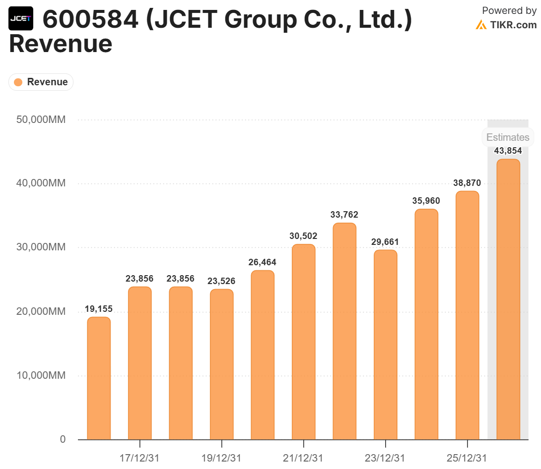
JCET is the largest packaging and testing leader in mainland China and one of the world’s top three OSAT companies, with a revenue of 43.8bn in 2026e. Its business covers communications, consumer electronics, high-performance computing, automotive electronics, industrial applications, memory, and AI-related fields. In recent years, JCET has continued to advance system-in-package, wafer-level packaging, 2.5D/3D packaging, fan-out packaging, and high-performance-computing-related packaging capability. For JCET, advanced packaging is not a single product line. It is the core direction for upgrading from a traditional packaging and testing company into a system-integration platform.
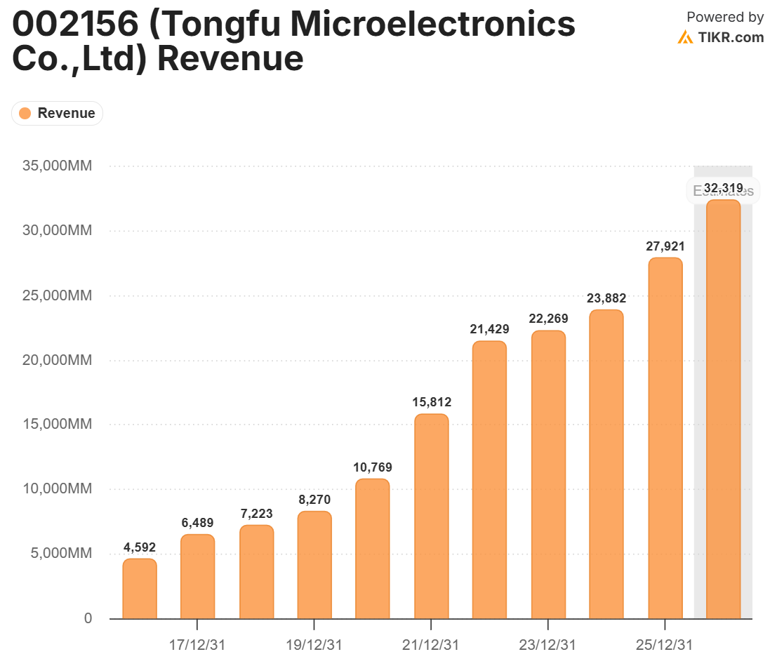
Tongfu Microelectronics has a path with stronger global participation. Its revenue is estimate to reach Rmb 32.3bn in 2026, up 6x in the past decade. It has maintained deep cooperation with AMD for a long time and has entered the international high-performance-computing supply chain through bases in Suzhou and Penang. Recent domestic reports noted that Tongfu Microelectronics is advancing multiple advanced packaging and wafer-level packaging expansions, with fundraising directed toward memory-chip packaging and testing, automotive and emerging applications, wafer-level packaging, high-performance computing, and communications projects. Reports also noted that Tongfu Penang’s 3nm multi-chip product packaging passed validation, while bumping and wafer testing entered smooth production with good yield performance.
This information deserves close attention. It shows that Chinese packaging and testing companies’ participation in global advanced packaging competition is not only about serving domestic customers. They are also entering the global high-end packaging system through overseas bases and international major customers. For China’s packaging and testing industry, validation by international customers is an important asset. Advanced packaging is ultimately not built by capacity alone. It is forged through high-end customers, highly complex products, long-term yield, and engineering capability.
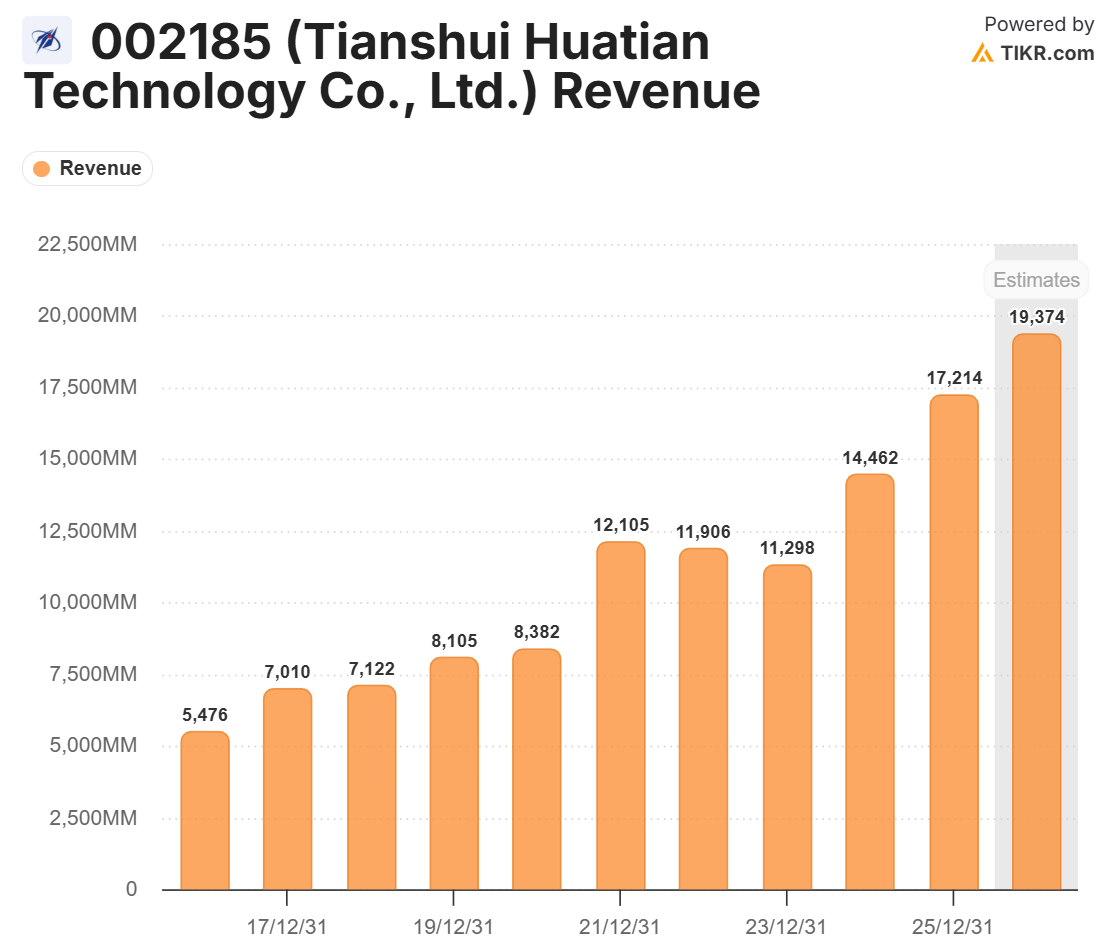
Huatian Technology represents another expansion path. Domestic reports noted that Huatian Technology is building Phase II of an advanced packaging and testing industrial base with a total investment of about RMB 10 billion. The project focuses on CPU/GPU/AI, memory chips, CPO, automotive electronics, and other markets, aiming to increase the share of advanced packaging technologies and accelerate mass production of 2.5D packaging and testing products. Huatian’s characteristics are broad base layout and wide product coverage. It is upgrading from traditional packaging and testing toward more advanced packaging formats.
SJ Semiconductor is one of the most important new samples in mainland China’s advanced packaging sector. It focuses more on 2.5D/3D advanced packaging, with most IPO fundraising directed toward three-dimensional multi-chip integrated packaging projects and ultra-high-density interconnect three-dimensional multi-chip integrated packaging projects. Domestic reports view SJ Semiconductor as one of mainland China’s more mature 2.5D advanced packaging platforms. This is crucial. 2.5D packaging is not a natural extension of traditional packaging and testing capability. It requires wafer-level processes, redistribution layers, interposers, micro-bumps, testing, yield control, and system-integration experience.
Together, JCET, Tongfu, Huatian, and SJ Semiconductor show that China’s advanced packaging is not starting from zero. It is upgrading from existing global packaging and testing capacity, domestic memory and AI demand, expanding capital expenditure, and customer validation.
3. AI Ties HBM, Chiplet, and Packaging Capability Together
The core of advanced packaging in the AI era is to organize multiple chips into a high-performance system. GPUs, CPUs, ASICs, HBM, I/O chips, chiplets, substrates, thermal structures, and power-delivery networks need to be recombined through packaging.
HBM is one of the most important pull factors. AI training requires massive memory bandwidth. Traditional DRAM is too far from compute chips, with insufficient bandwidth and poor energy efficiency. HBM stacks multiple layers of DRAM and connects them through TSV to push memory bandwidth much higher, then uses 2.5D packaging to connect with GPUs or AI accelerators. The bottleneck in this process is not only the DRAM die. It also lies in TSV, electroplating, thinning, temporary bonding, testing, yield, interconnect, substrates, and packaging integration.
Chinese memory companies and packaging/testing companies are both being pulled by this trend. CXMT’s DRAM expansion allows China to truly enter global DRAM competition for the first time, and it naturally raises the question of HBM-related capability construction. If platforms such as Tongfu, JCET, and SJ Semiconductor want to serve AI chips and high-bandwidth memory, they must enter more complex 2.5D/3D packaging, wafer-level processing, and high-density interconnect.
Chiplet is another major thread. Advanced process nodes are becoming increasingly expensive, and large chips face growing yield pressure. Many systems are beginning to split different functional modules into multiple chiplets, then connect them through advanced packaging. This turns packaging from a back-end protective structure into part of architectural design. Chip designers are no longer only designing one monolithic chip. They are designing a system composed of multiple chips. Packaging determines how these chips communicate, how they receive power, how they dissipate heat, how they are tested, and how costs are controlled.
This is why advanced packaging is becoming an important support for domestic AI chips. If Chinese AI chips are restricted on the most advanced process nodes, they need Chiplet, HBM, system-level packaging, and architectural optimization even more to improve usable performance. Advanced packaging cannot eliminate the process gap, but it can give system design more room for combination.
4. China’s Path Is Not a Simple Copy of CoWoS
The most representative case in global advanced packaging is TSMC’s CoWoS. It connects GPUs and HBM through silicon interposers and advanced packaging technology, becoming a key bottleneck in NVIDIA’s AI chip supply chain. The success of CoWoS shows that advanced packaging has become one of the most valuable manufacturing capabilities in global semiconductors.
But China’s path will not simply copy CoWoS.
On one hand, CoWoS is backed by TSMC’s long-term wafer-manufacturing capability, top-tier customers, EDA coordination, materials and equipment systems, and advanced process ecosystem. Mainland China cannot fully replicate this complete ecosystem in the short term. On the other hand, demand for advanced packaging in China is more complex: it includes domestic AI chips and high-performance computing, as well as memory, power semiconductors, automotive electronics, CPO, optical communications, consumer electronics, domestic GPUs, domestic CPUs, and military/industrial scenarios.
Therefore, China’s advanced packaging is more likely to develop through multiple parallel routes.
The first route is 2.5D/3D packaging. SJ Semiconductor, JCET, Tongfu, Huatian, and others are all advancing this direction to different degrees. It is suitable for high-performance computing, AI chips, Chiplet, and high-bandwidth-memory-related integration.
The second route is wafer-level packaging and fan-out packaging. Wafer-level packaging can improve integration density, reduce package size, and improve electrical performance, with room in RF, sensors, power management, consumer electronics, and some high-performance applications. Fan-out packaging helps achieve higher I/O density and thinner package structures.
The third route is SiP, or system-in-package. China has a huge market in consumer electronics, communications, automotive electronics, and IoT. SiP can integrate multiple functional chips, sensors, RF devices, and passive components inside one package. This route is not as glamorous as HBM/CoWoS, but it is very important for China’s electronics manufacturing ecosystem.
The fourth route is glass substrates and TGV. This direction has clearly heated up in domestic industry coverage over the past two months. Glass substrates have potential advantages such as low dielectric loss, dimensional stability, good flatness, suitability for high-density interconnect, and large-size packaging. TGV, or through-glass-via technology, is viewed as a possible important direction for next-generation advanced packaging substrates and panel-level packaging. WG Tech, Triumph Science & Technology, Crystal-Optech, Tongfu Microelectronics, BOE, and other companies have all been placed into this industrial-chain discussion by domestic reports.
The fifth route is advanced packaging equipment and materials. Hwatsing’s CMP, thinning, dicing, and edge-polishing equipment; ACM Research Shanghai’s electroplating, cleaning, and wet-process equipment; and materials from companies such as Dinglong, PhiChem, Hysol Huawei Electronics, and Darbond — including temporary bonding, packaging adhesives, underfill, molding compounds, photo-sensitive polyimide, and thermal interface materials — all form the support layer for advanced packaging.
Together, these routes show that China’s advanced packaging is not a single technology bet. It is a multi-layer industrial network built around AI, memory, domestic chips, and system-level integration.
5. TGV and Glass Substrates Bring Panel-Industry Experience into Semiconductor Packaging
Glass substrates are one of the most communicable directions in recent domestic advanced-packaging reporting. They attract attention because they connect China’s panel industry, glass processing, laser drilling, electroplated via filling, TGV, and advanced packaging.
Traditional semiconductor packaging relies more on organic substrates, silicon interposers, and wafer-level processing. The appeal of glass substrates is that they may offer new options in large size, high flatness, low loss, and high-density interconnect. AI chips are becoming larger, the number of HBM stacks is increasing, and package size is approaching physical and cost boundaries. Traditional substrates and silicon interposers are facing rising cost pressure. Glass substrates are therefore viewed as a potential new platform.
In domestic reporting, WG Tech has been repeatedly mentioned. Reports say it has advanced relatively quickly in TGV through-glass-via processes, showcased mass-producible 12-inch TGV glass substrates, and has entered small-batch delivery or sample-delivery stages for related products. Triumph Science & Technology, relying on specialty glass and the CNBM system, is advancing pilot production and customer testing in medium- and small-sized glass substrates, automotive chips, MEMS, optical communications, and other applications. BOE is also viewed as a potential force that could use panel production lines and glass-processing experience to enter semiconductor glass substrates.
The significance of this route is not only replacing one material with another. It may transfer China’s experience in glass processing, ultra-large-size substrates, clean manufacturing, yield control, equipment localization, and large-scale engineering from the panel industry into advanced packaging. China has accumulated extensive glass-substrate processing experience in LCD and OLED industries. If TGV and glass packaging substrates truly enter commercialization, this cross-industry capability transfer will be very important.
Of course, glass substrates are still at an early stage. They must solve many problems, including micro-hole processing, metallization, via filling, electroplating, warpage, coefficient-of-thermal-expansion matching, reliability, mass-production yield, cost, and customer process introduction. This is not yet a route that has definitively won. But for China, it is a technology path worth tracking because it has a strong connection with China’s existing panel and glass industrial base.
The most important thing about glass substrates is that they pull advanced packaging out of the traditional semiconductor packaging and testing industry and toward a broader combination of industrial capabilities.
6. Advanced Packaging Materials Are Becoming Invisible Bottlenecks
The more complex advanced packaging becomes, the more important materials become. Traditional packaging materials mainly protect chips, connect circuits, and provide mechanical support. In the AI era, advanced packaging materials begin to carry higher requirements: high-density interconnect, thermal management, stress control, ultra-thin wafer handling, temporary bonding, hybrid bonding, underfill, low warpage, low dielectric loss, and long-term reliability.
In domestic reporting, advanced packaging materials are divided into several key directions.
The first is temporary bonding materials. During TSV, wafer thinning, and 3D stacking, wafers need to be temporarily fixed to carriers. After thinning, etching, electroplating, cleaning, and other processes are completed, they are debonded. Materials must resist high temperature, have low residue, high cleanliness, and easy release, while avoiding wafer damage. Dinglong and PhiChem are among the companies placed into this direction by domestic reports.
The second is underfill and molding materials. There are many tiny solder joints between chips and substrates, and they must withstand thermal cycling, mechanical stress, and long-term operation. Underfill protects solder joints, disperses stress, and improves reliability; molding compounds protect chip structures and control warpage. Hysol Huawei Electronics, Darbond, PhiChem, Novoray, and other companies are related to this material chain.
The third is photo-sensitive polyimide, packaging photoresist, and RDL materials. Advanced packaging requires redistribution layers, insulation layers, and high-density pattern transfer. These materials directly affect packaging interconnect density and reliability. If Chinese materials companies can pass customer validation in these directions, they can enter higher-value fields than traditional packaging materials.
The fourth is thermal-management materials. AI chips are consuming more and more power. Packaging must not only connect chips; it must also handle heat. Thermal interface materials, heat-dissipation materials, and low-thermal-resistance package structures are becoming part of system performance. If advanced packaging cannot solve thermal problems, chip design performance cannot be released.
The hardest part of materials is the long qualification cycle. Packaging materials must go through high-temperature, high-humidity, thermal shock, long-duration operation, mechanical stress, warpage, and reliability testing. Being able to package a chip is only the first step. The real threshold is whether expensive AI chips can operate stably over the long term.
7. Advanced Packaging Equipment Is Gaining New Demand
Advanced packaging needs not only packaging and testing companies, but also equipment companies. Earlier analyses of China’s semiconductor equipment have already mentioned that Hwatsing, ACM Research Shanghai, NAURA, Piotech, AMEC, and other equipment companies are approaching advanced-packaging demand to different degrees.
Advanced packaging needs CMP, thinning, dicing, edge polishing, electroplating, cleaning, temporary bonding, debonding, inspection, metrology, placement, bonding, molding, and testing equipment. Many pieces of equipment used to sit near the boundary between front-end and back-end processes. Now, because of 2.5D/3D packaging, HBM, and Chiplet, they are becoming much more important.
Hwatsing’s CMP, thinning, dicing, and edge-polishing equipment directly serve wafer-level processing and 3D integration demand in advanced packaging. ACM Research Shanghai’s electroplating and cleaning equipment can enter TSV, electroplating, wet processing, and advanced packaging processes. If domestic equipment companies can pass advanced-packaging customer validation, they may obtain a growth path different from advanced front-end process nodes.
This is also the special value of advanced packaging for China’s semiconductor industry. It connects equipment, materials, packaging/testing, memory, and AI chips. An advanced packaging project is not only packaging-factory expansion. It also pulls electroplating equipment, cleaning equipment, CMP equipment, thinning equipment, temporary bonding materials, underfill materials, packaging substrates, and testing equipment.
Advanced packaging is becoming an intersection point for China’s semiconductor industrial chain.
8. Global Participation Should Be Viewed in Layers
China’s current global participation in advanced packaging is best understood as layered participation.
The first layer is the global OSAT system. JCET, Tongfu, and Huatian are already important companies in the global packaging and testing market, with overseas customers, overseas bases, and roles in international supply chains. Tongfu, in particular, has actual participation in the global high-performance-computing packaging supply chain through AMD-related business and its Penang base.
The second layer is mainland advanced packaging platforms. Companies such as SJ Semiconductor are more focused on building capabilities in mainland China around 2.5D/3D packaging, three-dimensional multi-chip integration, and ultra-high-density interconnect. They mainly serve domestic high-end chips, domestic computing power, and local supply-chain security needs. Global participation at this layer is not necessarily reflected in the number of overseas customers, but in whether they can support China’s local high-performance chip ecosystem.
The third layer is the materials and equipment supply chain. Dinglong, PhiChem, Hysol Huawei Electronics, Darbond, Hwatsing, ACM Research Shanghai, WG Tech, and others may enter global technology trends through advanced packaging materials, equipment, and glass substrates. They do not necessarily face final AI chip customers directly, but if they pass validation in key materials and equipment, they will become foundational participants in the advanced packaging ecosystem.
The fourth layer is the high-end ecosystem where China still has obvious shortages. In the highest-end CoWoS-level capacity, the most advanced HBM packaging, silicon-interposer ecosystems, binding with global top-tier AI customers, advanced packaging EDA/design coordination, high-end substrates, thermal management, and large-scale yield control, China still has gaps with ecosystems related to TSMC, ASE, Amkor, Samsung, and SK hynix.
This layered judgment is important. China’s advanced packaging is neither simply behind nor fully caught up. It is forming capabilities in some links, participating in global supply chains in some links, serving domestic substitution in some links, and still needing long-term catch-up in other links.
9. The Strategic Significance of China’s Advanced Packaging
The strategic significance of advanced packaging for China’s semiconductor industry can be understood in three layers.
First, it is a performance amplifier for domestic AI chips. Today’s AI competition is not only chip design competition, but also system-integration competition. If Chinese AI chips cannot obtain enough advanced packaging capability, it will be difficult to solve HBM connection, Chiplet integration, heat dissipation, bandwidth, and power-consumption problems. Advanced packaging will directly affect whether domestic AI chips can scale into training and inference scenarios.
Second, it is a realistic compensation path under front-end process constraints. Advanced packaging cannot replace the most advanced process nodes, but it can improve the system performance of mature-node or slightly less-advanced chips through Chiplet, heterogeneous integration, HBM, and system-level optimization. The market discussion around Huawei’s “Tao’s Law” points to exactly this: the rising importance of system-level organizational capability.
Third, it is an intersection point of China’s industrial system capability. Advanced packaging requires packaging and testing companies, wafer fabs, memory companies, equipment companies, materials companies, substrate makers, glass companies, testing companies, chip design companies, and system customers to participate together. This kind of complex organization is precisely an area where Chinese manufacturing has relative strengths. If China can organize these links, advanced packaging may become one of the semiconductor areas that best reflects system capability.
This does not mean China can bypass all front-end bottlenecks. Advanced packaging is not magic. Without good enough chips, memory, substrates, materials, and design tools, packaging cannot create miracles by itself. But it does provide a more realistic, more engineering-oriented, and more China-advantage-aligned breakthrough direction.
Conclusion: Advanced Packaging Is Becoming China’s System-Level Semiconductor Test Field
The real significance of advanced packaging is that China’s semiconductor industry is beginning to enter system-level computing competition. AI chips no longer need only single-chip manufacturing capability. They require coordination among GPUs/ASICs, HBM, Chiplet, substrates, materials, equipment, testing, thermal management, and system customers.
Chinese companies have already begun entering this competition. JCET, Tongfu, Huatian, and SJ Semiconductor are upgrading from traditional packaging and testing toward 2.5D/3D, wafer-level packaging, Chiplet, high-performance computing, and AI-related packaging. WG Tech, Triumph Science & Technology, BOE, and others have made glass substrates and TGV new directions to watch. Dinglong, PhiChem, Hysol Huawei Electronics, Darbond, and other materials companies are entering temporary bonding, underfill, molding compounds, photo-sensitive polyimide, and thermal-management materials. Hwatsing and ACM Research Shanghai are entering this new battlefield through CMP, thinning, electroplating, cleaning, and advanced packaging equipment.
This network is still incomplete. China still lacks a mature global top-tier platform like TSMC’s CoWoS, and it still faces multiple bottlenecks in high-end customers, yield, HBM integration, substrates, thermal management, materials, and equipment. But advanced packaging has already become one of the most important directions to watch in China’s semiconductor industry, because it connects China’s existing packaging and testing scale, memory progress, AI demand, materials industry, equipment breakthroughs, and system-integration capability.
The core of China’s advanced packaging is not “back-end upgrading.” It is pushing the chip industry from single-point process competition into system-organization capability competition.
In the AI era, whoever can organize compute chips, memory chips, packaging substrates, materials, equipment, and thermal systems into a mass-producible, verifiable, deliverable system will possess more real computing-manufacturing capability. China’s advanced packaging has not yet completed its breakthrough, but it has already entered the real test field.
Source note: This essay is based on recent Chinese industry-media reports and company coverage from Jiwei, Semiconductor Industry Observation, EET China, Sina Finance, Securities Times, CLS, Eastmoney, and related domestic reporting on China’s advanced packaging companies, HBM/Chiplet packaging, 2.5D/3D integration, glass substrates/TGV, advanced packaging equipment, and packaging materials. All translations of short quoted phrases are my own.
If this framework helps you understand China, industrial power, state capacity, capital, technology, and global order beyond the usual headlines, please consider subscribing to China as a System.
A like, restack, comment, or share also helps this work reach more readers.
For a full guide to the publication and its main research series, start here: China as a System: Publication Map.
