
Inside China’s Semiconductor Materials Catch-Up
The Hardest Underlying Battlefield of China’s Chip Localization

The localization of semiconductor materials is more hidden—and in many ways more unforgiving—than the localization of equipment. Equipment can be seen. Materials must prove themselves gradually through purity, consistency, defect control, long-term validation, and customer trust.
This essay is part of China Industry Signals.
Executive Summary
China’s semiconductor-materials industry is entering a deeper stage of localization, driven by domestic fab expansion, DRAM capacity growth, advanced packaging, and supply-chain security pressure.
The strongest industrial signal is the shift from “material availability” to fab-level qualification, batch stability, purity control, defect reduction, and customized joint development with customers.
Silicon wafers, wet electronic chemicals, CMP materials, electronic specialty gases, sputtering targets, photoresists, precursors, and advanced-packaging materials are moving at very different speeds.
China has made faster progress in wet electronic chemicals, CMP slurry/pads, selected sputtering targets, electronic gases, and some packaging materials, while high-end photoresists, advanced precursors, high-purity components, and EUV-related materials remain hard bottlenecks.
The rise of CXMT, YMTC, SMIC, Hua Hong, power-semiconductor fabs, and advanced-packaging platforms is turning materials localization from a policy slogan into a production-line validation process.
The real measure of China’s semiconductor-materials catch-up is not whether a domestic supplier can make a material once, but whether it can deliver stable batches repeatedly inside demanding fabs.

Strange Peaks and Layered Ridges (层峦奇峰), by Liu Haisu (刘海粟), 1896–1994
Its rising peaks, layered structure, and powerful vertical momentum mirror the core argument of this essay.
Materials Are the More Hidden Semiconductor Battlefield
In the semiconductor industry, equipment is the easiest to see. Lithography machines, etching tools, deposition equipment, and ion implanters all have clear physical forms, and capital markets and the media can easily turn them into stories of technological breakthrough. Materials are different. They often enter the production line as liquids, gases, powders, films, targets, wafers, resins, slurries, and additives. Their visibility is low, but their impact on yield, reliability, and process limits is enormous.
A wafer fab consumes large amounts of materials every day. Silicon wafers are the starting point of chip manufacturing. Photoresist determines pattern transfer. Electronic specialty gases participate in etching, deposition, cleaning, and doping. Wet electronic chemicals continuously clean and etch wafer surfaces. CMP slurries and polishing pads determine planarization quality. Sputtering targets are used for metal thin films. Precursors determine the quality of CVD and ALD films. Advanced packaging materials affect the reliability of Chiplets, HBM, and system-level packaging.
These materials are not purchased once like equipment. They are continuously consumed, continuously validated, and continuously affecting yield.
The cruelest part of semiconductor materials is that customers do not only ask whether something can be made. They look at purity, metal impurities, particles, batch consistency, storage stability, supply continuity, process window, defect rate, and compatibility with equipment and process recipes. Many materials can be produced in the laboratory and run through pilot lines, but once they truly enter a wafer fab, trace impurities, batch fluctuations, storage and transportation conditions, residues, or interface reactions can affect the entire process flow.
This is why semiconductor materials localization is slower than the outside world imagines. It is not a single-point breakthrough problem. It is a long-term trust problem. Wafer fabs will not easily replace critical materials simply because of supply-security pressure. Once a material goes wrong, it may cause an entire batch of wafers to be scrapped. It may also create reliability risks in customers’ end products. For advanced processes and memory chips, materials stability itself is part of process capability.
The stage China’s semiconductor materials industry is now entering is precisely the movement from “usable” to “stably usable,” from “sample validation” to “batch introduction,” and from “domestic substitution” to “joint development with customers.”
China Is Already One of the World’s Largest Demand Sites for Materials
The acceleration of China’s semiconductor materials localization first comes from changes on the demand side. Mainland China is already one of the most important semiconductor materials markets in the world. Domestic wafer fab expansion, the rise of the memory industry, continuous investment in mature nodes, growth in power semiconductors, and rising demand for advanced packaging are all expanding materials consumption.
Industry reports have noted that in 2024, the mainland Chinese semiconductor materials market was about $20.5 billion, up 13.89% year on year, accounting for about 28.40% of the global market, making it one of the world’s largest and most important regional markets. Another report on wet electronic chemicals noted that as newly built domestic wafer fabs enter a peak commissioning period, demand for ultra-high-purity wet electronic chemicals is growing rapidly. China’s wet electronic chemicals market is expected to grow from RMB 10.062 billion in 2020 to nearly RMB 18.183 billion in 2026, with a compound growth rate of about 12.6%.
Behind these numbers lies a very important industrial fact: Chinese materials companies, for the first time, have a sufficiently large domestic customer site.
One of the greatest difficulties for the materials industry in the past was the lack of sufficiently high-intensity customer validation scenarios. Materials suppliers must be bound to wafer fabs over the long term, enter customer process flows, and go through lab trials, pilot runs, sample delivery, validation, substitution, batch supply, abnormality handling, and next-generation formula development. Without enough wafer fabs, enough production lines, and long enough process feedback, materials companies struggle to truly mature.
Now, CXMT, YMTC, SMIC, Hua Hong, Nexchip, Silan Micro, CR Micro, NCE Power, Wingtech, San’an, advanced packaging plants, and a large number of power semiconductor production lines are jointly providing these scenarios. They are not simply buying domestic materials. They are building a local materials validation system.
The first essay on the CXMT chain group discussed the equipment validation field. The materials sector follows a similar logic. CXMT’s DRAM expansion will not only drive validation demand for etching tools, deposition equipment, cleaning tools, and CMP equipment. It will also drive validation demand for silicon wafers, electronic specialty gases, wet electronic chemicals, CMP materials, photoresist supporting materials, precursors, targets, and packaging materials. Memory production lines have strong process repeatability, large scale, and high yield sensitivity, making them an extremely demanding examination site for materials suppliers.
What China’s semiconductor materials industry needs most is not only subsidies and papers. It needs this kind of examination.
Silicon Wafers: The First Substrate of Chip Manufacturing
Silicon wafers are the starting point of semiconductor manufacturing. Without high-quality silicon wafers, there can be no subsequent lithography, etching, deposition, or doping. Silicon wafers may look like the most basic material, but they impose extremely high requirements on purity, crystal defects, flatness, particles, metal contamination, warpage, oxygen content, dimensional stability, and surface quality.
12-inch silicon wafers are especially critical. Advanced logic, memory, and most mainstream wafer manufacturing depend on 12-inch wafers. For a long time, the global large-wafer market has been dominated by companies from Japan, South Korea, Taiwan, and Germany. Shin-Etsu Chemical, SUMCO, GlobalWafers, Siltronic, and SK Siltron all have strong customer lock-in and long-term process accumulation.
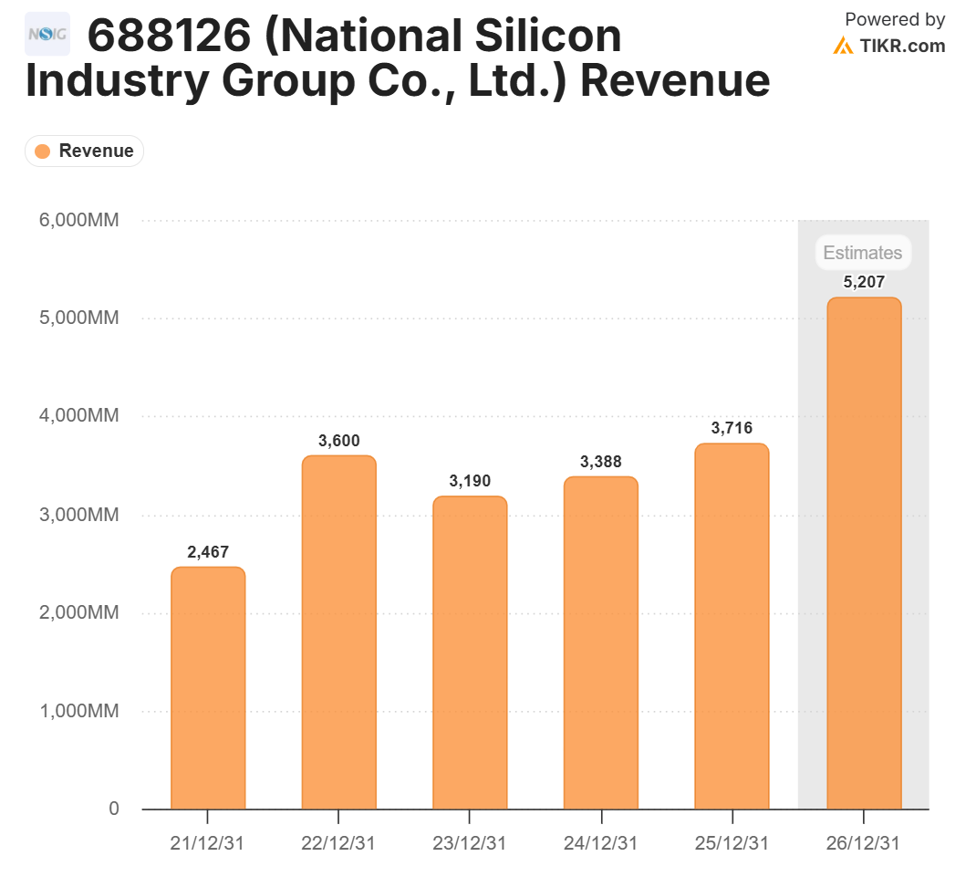
Chinese companies have already made progress in silicon wafers. National Silicon Industry Group, Zhonghuan Advanced, Leon Micro, and Thinkon Semiconductor are gradually entering the supply chains of domestic wafer fabs. The difficulty of 12-inch large wafers lies not only in crystal pulling and slicing, but in batch stability. What wafer fabs need is long-term stable supply. One qualified batch is not enough. Every batch must be stable. Silicon wafer defects travel through the entire process flow. Any crystal defect, metal contamination, surface defect, or flatness problem may be amplified in later processes.
Silicon wafer localization also carries strategic significance. It sits at the most upstream point of the materials chain and determines the basic supply security of wafer fabs. The faster China’s wafer fabs expand capacity, the greater the demand for 12-inch silicon wafers. If local silicon wafer companies can enter batch supply for more customers, they will gain stronger feedback loops and scale effects.
But silicon wafers are not a problem that has already been fully solved. High-end 12-inch silicon wafers, epitaxial wafers, SOI, SiC substrates, GaN substrates, and InP substrates all have their own bottlenecks. Advanced logic and memory impose higher requirements on silicon wafers, while compound semiconductors raise another set of challenges for silicon carbide, gallium nitride, and other substrates. China’s silicon wafer industry has already formed basic capability, but high-end products still require long-term iteration.
Photoresist: One of the Hardest Chemical Systems to Localize
Among all semiconductor materials, photoresist is the easiest for the public to understand and one of the hardest to truly localize. Photoresist directly participates in pattern transfer and is the core consumable of the lithography process. It is not a simple chemical. It is a complex system composed of resins, photoacid generators, solvents, additives, and supporting materials. It must be highly matched with the lithography machine, mask, exposure wavelength, developer, bottom anti-reflective coating, etching process, and the customer’s specific process flow.
China’s photoresist industry is breaking through in layers. Recent industry reports have noted that China’s semiconductor photoresist industry has already gone through multiple stages, with KrF localization rising, ArF entering small-batch introduction, and EUV pre-research beginning. This judgment is accurate. China is not without photoresist capability, but high-end photoresist remains one of the most difficult segments.
From a product-level perspective, g-line and i-line photoresists are relatively mature, KrF photoresists are expanding validation and introduction, ArF dry and immersion photoresists remain at a higher-difficulty stage, and EUV photoresist is still one of the highest-threshold materials globally. The difficulty of high-end photoresist is not only the formula. It is the extremely long customer validation cycle. Whether a photoresist formula can enter mass production depends on resolution, line-edge roughness, sensitivity, etch resistance, defect rate, metal-ion content, coating uniformity, development window, and long-term batch stability.
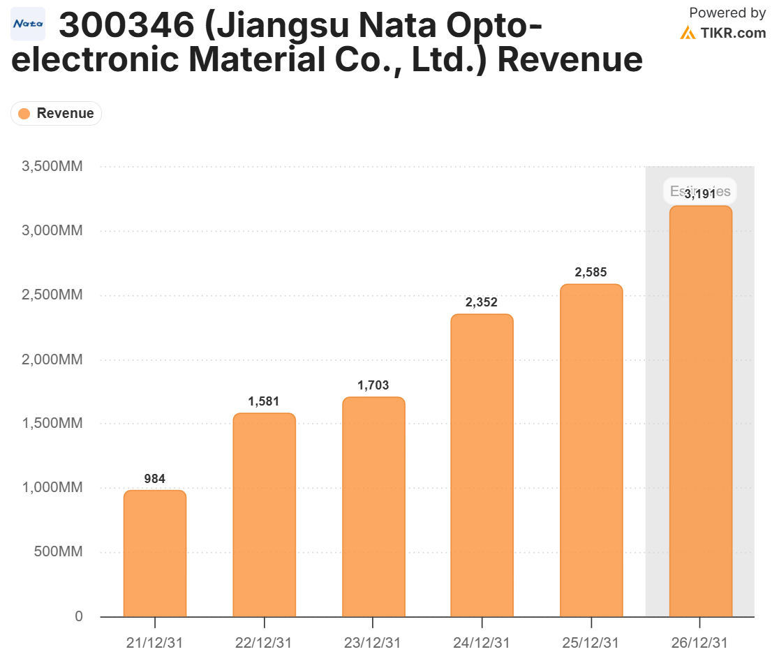
Companies such as Nata Opto-electronic, Jingrui Electronic Materials, Red Avenue New Materials, Shanghai Sinyang, Hengkun New Materials, Dinglong, and Aisen are all advancing photoresists and supporting materials in different segments. More specifically, beyond photoresist itself, there are also supporting materials such as SOC, BARC, developers, strippers, photoinitiators, photosensitive polyimide, and advanced packaging photoresists. In many cases, supporting and auxiliary materials are equally critical.
The hardest part of photoresist localization is that it requires joint validation across wafer fabs, lithography machines, masks, development, etching, and inspection. Materials companies cannot achieve a breakthrough in isolation from customer production lines. Even if laboratory performance reaches the required level, the material still has to go through repeated customer testing. Once a customer switches photoresist, the subsequent process window may also need to be adjusted. That cost is very high.
So photoresist localization will not be a story that is suddenly completed. It will likely advance through a layered path: KrF expands first, ArF is gradually introduced, advanced packaging photoresists break through faster, and EUV remains a long-term pre-research effort. It is also one of the segments in China’s semiconductor materials localization that best reflects long-termism.
Electronic Specialty Gases: The Invisible Bloodstream Running Through the Entire Production Line
Electronic specialty gases are the “gas materials system” of semiconductor manufacturing. They participate in etching, deposition, cleaning, ion implantation, lithography support, doping, and chamber treatment. Fluorocarbon gases, silane, ammonia, chlorine, nitrogen trifluoride, xenon, neon, helium, arsine, phosphine, diborane, and other gases all play roles in different processes.
The core of electronic specialty gases is not ordinary industrial gas. It is ultra-high purity, ultra-low impurities, stable supply, and process compatibility. Semiconductor-grade gases require extremely high purity. Trace amounts of moisture, oxygen, metal impurities, or particles can affect the process. Gas supply also involves cylinders, valves, pipelines, gas cabinets, transportation, on-site safety, and stable delivery.
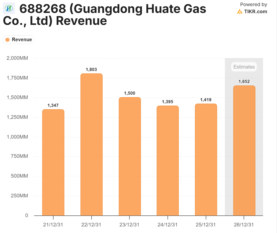
China has already built a certain foundation in electronic specialty gas localization. Companies such as Huate Gas, Jinhong Gas, Nata Opto-electronic, Yoke Technology, Haohua Technology, and Heyuan Gas are advancing domestic substitution across different products. Industry reports often note that the localization rate of electronic specialty gases is already higher than that of high-end photoresists, but gaps remain in high-end varieties, specialty gases, and advanced-node supporting products.
Electronic specialty gases have one special advantage: they are deeply bound to customers. Once a wafer fab completes qualification and begins stable use, the supplier relationship tends to be durable. Switching gas suppliers also brings process risk. If domestic companies can enter customer systems, they may have opportunities to increase their share through product-category expansion.
But electronic specialty gases also have a special challenge: they are not about a single-product breakthrough. They require integrated capabilities in safety, purification, analysis, packaging, supply chain, and field service. Gases must be delivered stably over the long term, and customer production lines cannot tolerate supply interruptions. Suppliers need both chemical synthesis and purification capabilities, as well as semiconductor customer-service capabilities.
Electronic specialty gases show that materials localization is not merely about “making one material.” It also includes purification systems, testing systems, transportation systems, storage systems, on-site supply systems, and customer qualification systems. A country’s semiconductor materials capability is often hidden inside these seemingly ordinary links.
Wet Electronic Chemicals: The High-Purity Battlefield Inside Cleaning and Etching
Wet electronic chemicals are one of the faster-moving but still underestimated categories in China’s semiconductor materials localization. They include electronic-grade hydrofluoric acid, sulfuric acid, nitric acid, hydrochloric acid, ammonia water, hydrogen peroxide, phosphoric acid, etchants, developers, strippers, cleaning solutions, and related products. They are widely used in wafer cleaning, wet etching, development, stripping, and surface treatment.
Wet electronic chemicals are characterized by large usage volumes, high purity requirements, and high process frequency. Every batch of wafers in a fab goes through multiple cleaning and wet-processing steps. Material purity, metal-ion control, particle control, stability, and supply continuity directly affect yield.
Industry reports show that China’s wet electronic chemicals market is growing rapidly and is expected to approach RMB 18.183 billion in 2026. This market growth comes from the commissioning and expansion of domestic wafer fabs, as well as the acceleration of materials localization. Companies such as Xingfu Electronic, Jingrui Electronic Materials, Jianghua Micro, Shanghai Sinyang, PhiChem, and GreenDa are advancing localization across different wet electronic chemicals and supporting materials.
Wet electronic chemicals have localized relatively faster partly because China already has a powerful basic chemical industry. China has vast chemical capacity, fine-chemical talent, engineering scale-up capability, and cost advantages. But semiconductor-grade chemicals are not ordinary chemicals. Their difficulty lies in extreme purification, impurity control, clean production, packaging and transportation, and customer qualification. Ordinary chemical capability must be upgraded into electronic-grade materials capability.
This is a miniature version of the transformation of China’s materials industry. China was historically strong in bulk chemicals and industrial materials. Now it must move into semiconductor materials that are ultra-high-purity, low-defect, traceable, and customer-customized. This is not a simple capacity upgrade. It is an upgrade of the quality system, inspection system, and customer co-development system.
CMP Materials: Slurries and Pads Determine Planarization Quality
CMP materials include slurries, polishing pads, cleaning solutions, conditioning discs, and related products. Together with CMP equipment, they determine the planarization quality of the wafer surface. The more advanced processes and advanced packaging develop, the more critical CMP becomes. Copper interconnects, tungsten, dielectric layers, STI, TSV, hybrid bonding, and 3D packaging all require different CMP material systems.
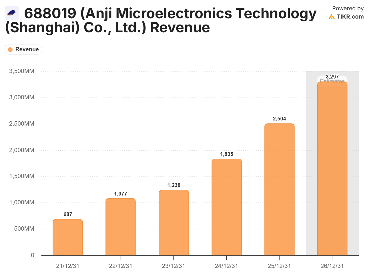
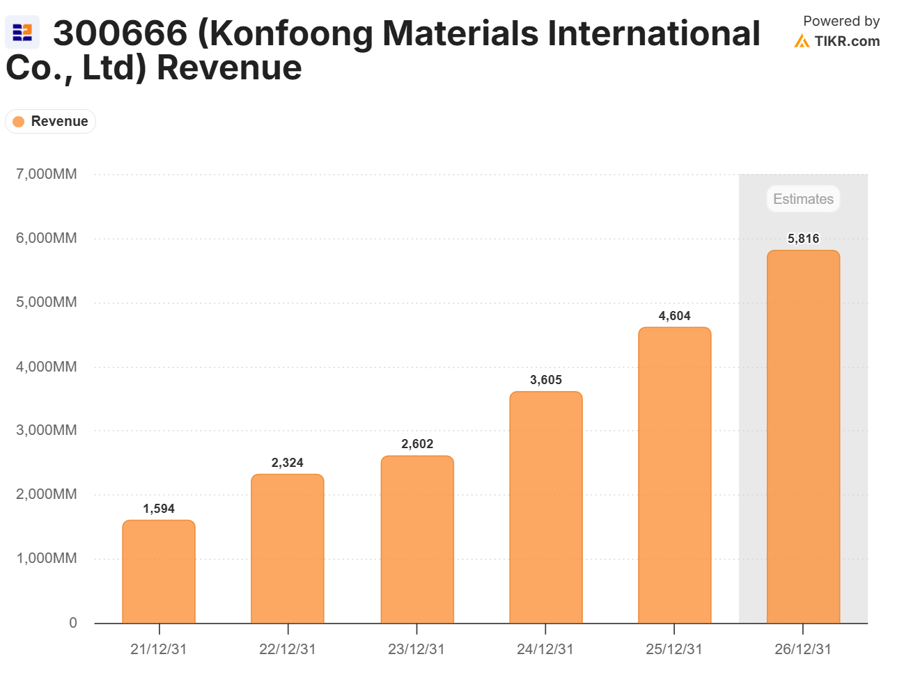
Anji Technology is a representative Chinese company in CMP slurries, while Dinglong has made visible progress in CMP polishing pads and related materials. The difficulty of CMP materials lies in the fact that they are highly process-dependent formulation materials. Slurries must simultaneously consider chemical reaction rate, mechanical removal rate, selectivity, particles, defects, surface roughness, corrosion control, and cleaning residues. Polishing pads must balance hardness, pore structure, lifetime, stability, and removal uniformity.
CMP materials localization has one important feature: it is more likely to achieve breakthroughs through joint development with local customers. Different customers, different tools, and different processes all have different requirements for slurries and polishing pads. Materials suppliers need to work with wafer fabs to adjust formulas, run processes, examine defects, and conduct reliability testing. This process is very slow, but once it succeeds, customer stickiness is high.
Advanced packaging is opening new space for CMP materials. Hybrid bonding, TSV, wafer thinning, redistribution layers, and 3D integration all require higher-precision planarization materials. The faster China’s advanced packaging develops, the more opportunities CMP materials companies will have to enter new process routes.
CMP materials show an important trend: China’s semiconductor materials localization does not have to break through only from the most advanced logic processes. It can also build capability through memory, mature nodes, power semiconductors, and advanced packaging, and then extend toward higher-end applications.
Sputtering Targets and Precursors: Materials Control Behind Thin-Film Quality
Sputtering targets and precursors are critical materials in thin-film formation. PVD equipment requires sputtering targets, while CVD and ALD equipment require precursors. Thin-film quality depends not only on equipment, but also on material purity, stability, reaction characteristics, and supply consistency.
Sputtering targets are mainly used for metal thin films and interconnect materials. High-purity aluminum, copper, titanium, tantalum, tungsten, cobalt, nickel, molybdenum, and other targets have important applications in semiconductor manufacturing. Companies such as Jiangfeng Electronics, Grinm Advanced Materials, and Ashine are advancing domestic substitution in sputtering targets. The difficulty of targets lies in ultra-high purity, grain structure, microstructural uniformity, bonding technology, dimensional control, and customer qualification. Advanced processes impose stricter requirements on targets. Any impurity or structural non-uniformity may affect thin-film quality.
Precursors are a more hidden and more advanced category of materials. ALD and CVD processes rely on precursors to form extremely thin, uniform, and controllable films. The more advanced semiconductor processes become, the higher the requirements for precursors. GAA, multilayer stacking, 3D DRAM, advanced memory, advanced packaging, and new material systems all require more complex precursors. Precursor materials must not only be able to react. They also need suitable volatility, thermal stability, reaction selectivity, low residue, low contamination, and safe delivery characteristics.
Precursor localization is especially difficult because it sits between chemical synthesis, equipment delivery, and process application. Materials companies must understand equipment and processes. They cannot simply make chemicals. A report by EET China on precursor materials noted that precursor localization is not only about supply-chain security, but also determines the process limits and yield ceiling of advanced nodes. Beyond single-point technological breakthroughs, deep coordination with precision delivery systems and the systematic capability to move from basic research to industrial validation are the key to solving the “final barrier.”
This sentence is highly accurate. The more advanced a material becomes, the less it can be separated from equipment and process. If a precursor cannot be delivered stably, cannot form the desired film on customer equipment, and cannot control impurities and residues over the long term, it cannot be considered a real breakthrough. It requires joint validation by materials companies, equipment companies, and wafer fabs.
Advanced Packaging Materials Are Becoming a New Growth Point
Advanced packaging is redefining demand for semiconductor materials. In the past, packaging materials mainly included lead frames, substrates, solder balls, epoxy molding compounds, underfill, DAF films, and similar products. Now, Chiplets, 2.5D/3D packaging, HBM, hybrid bonding, RDL, TSV, wafer-level packaging, and panel-level packaging are making packaging materials much more advanced.
Advanced packaging requires more high-performance resins, dielectric materials, temporary bonding materials, photosensitive polyimide, underfill materials, packaging photoresists, electroplating solutions, solders, thermal interface materials, and high-end substrate materials. AI chips and high-performance computing are driving demand for larger chips, larger packages, higher bandwidth, and stronger heat dissipation, which will also increase material complexity.
China has a special opportunity in advanced packaging materials. The more visible the constraints on advanced lithography become, the more important advanced packaging and system-level integration become. Although packaging materials also have high-end bottlenecks, compared with extreme front-end materials such as EUV photoresists, some advanced packaging materials are more likely to achieve faster breakthroughs through joint development with local customers.
Companies such as Dinglong, PhiChem, Aisen, Qiangli New Materials, Red Avenue New Materials, Shanghai Sinyang, and Anji Technology are all advancing in areas such as advanced packaging materials, photosensitive polyimide, CMP materials, electroplating solutions, packaging photoresists, epoxy molding compounds, and thermal materials. This field may become one of the areas where Chinese materials companies are most likely to form differentiated growth.
The significance of advanced packaging materials is that they connect semiconductor manufacturing, packaging, AI chips, power devices, and system integration. They are not low-end back-end materials in the traditional sense. They are part of the improvement of system performance.
The Real Difficulty of Materials Localization Is Customer Qualification
All semiconductor materials localization eventually returns to one question: customer qualification.
Equipment introduction is difficult. Materials qualification is just as difficult. Once a material enters a wafer fab, it must go through strict testing. Customers look not only at basic specifications, but also at long-term stability, defect performance, compatibility with existing equipment and processes, batch consistency, supply continuity, and abnormality-handling capability. The validation cycle for many materials may last one year or even longer. The more critical the material, the more cautious the customer.
The most painful stage for domestic materials companies is often not R&D, but validation. After samples are delivered, customer testing is slow. After tests are passed, the substitution ratio is small. After small-batch introduction, long-term observation is still required. If an abnormality appears, validation may have to restart. This process consumes both capital and patience.
But once qualification is passed, materials companies gain very strong customer stickiness. Wafer fabs do not easily change materials. Materials and processes are deeply bound together, and supplier relationships are long-term. This is also why once semiconductor materials companies enter major customer supply chains, their commercial value continues to be released.
Chinese materials companies are now going through this process. They must move from the “domestic substitution list” into the “customer procurement system,” and then from the “customer procurement system” into “long-term supply for critical processes.” Every step in between is difficult, and every step is more valuable.
The West Underestimates the Industrial Soil Beneath China’s Materials Sector
The Western world tends to underestimate China’s semiconductor materials industry for two reasons.
First, it is accustomed to understanding semiconductor competition as a contest over a few high-end tools and advanced nodes, while ignoring materials — a low-visibility, long-cycle, highly engineering-intensive segment. Materials do not spread through public discourse as easily as lithography machines, nor do they attract attention the way AI chips do. But they are the underlying consumables of the entire production line.
Second, it underestimates China’s iterative capability once chemicals, materials, manufacturing, and customer-site engineering are combined. China is not building materials from zero. China has one of the world’s most complete chemical systems, as well as a vast industrial foundation in new energy, panels, photovoltaics, batteries, electronics manufacturing, and fine chemicals. Semiconductor materials are indeed more advanced, but they are not an isolated island that appears out of nowhere. They are built on top of a much larger materials-industrial system.
This does not mean China will easily break through in semiconductor materials. High-end photoresists, EUV materials, advanced precursors, ultra-high-purity materials, some electronic specialty gases, high-end silicon wafers, and high-end packaging materials remain difficult. But China’s advantage is that downstream customers are forming, production-line demand is expanding, and materials companies have opportunities to iterate repeatedly in real processes.
Breakthroughs in semiconductor materials will not be completed suddenly like a software release. They are more like long-term industrial domestication: materials enter customer sites, expose problems, adjust formulas, control impurities, improve batch stability, and then enter the next round of validation. This process is slow, but once it works, it creates thick industrial barriers.
China’s Semiconductor Materials Capability Map Is Becoming Thicker
China’s semiconductor materials localization cannot be summarized by one overall localization rate. It is more like a layered capability map.
The first layer includes segments that have already built a relatively strong foundation for domestic substitution, including some wet electronic chemicals, CMP slurries and polishing pads, some targets, some electronic specialty gases, some packaging materials, and some silicon wafer products.
The second layer includes segments that are accelerating introduction and customer validation, including KrF photoresists, some ArF photoresists, advanced packaging photoresists, high-end wet electronic chemicals, precursors, advanced packaging materials, 12-inch silicon wafers, SiC substrates, and some high-end targets.
The third layer includes segments that remain highly difficult, including EUV photoresists, some advanced ArF immersion photoresists, high-end precursors, key materials with extremely high purity requirements, advanced-node supporting materials, some high-end electronic specialty gases, and certain specialty packaging materials.
This unevenness is entirely normal. Materials localization has always advanced layer by layer. What matters most is that Chinese materials companies have begun moving from low-end consumables, ordinary chemicals, and auxiliary materials into materials that are more critical, higher-purity, more customized, and more deeply tied to specific processes.
The thickening of this capability map matters more than any single breakthrough. It shows that China’s semiconductor industry is beginning to form a more complete feedback system among equipment, materials, components, processes, customers, and capital expenditure.
Conclusion: Materials Localization Is the Real Underlying Resilience of the Semiconductor Industry
Semiconductor materials are not as dazzling as lithography machines, but they are closer to the underlying resilience of a country’s semiconductor industry. Equipment determines process capability. Materials determine process stability. Without stable materials supply, even the most advanced equipment cannot sustain mass production. Without customer validation, domestic materials remain trapped at the sample stage. Without batch consistency, domestic substitution cannot enter critical processes.
China’s semiconductor materials industry is entering a more real stage. Wet electronic chemicals, CMP materials, electronic specialty gases, silicon wafers, targets, photoresists, precursors, and advanced packaging materials are all advancing at different speeds. They will not break through at the same time, and they will not develop evenly. High-end photoresists, EUV materials, advanced precursors, and some ultra-high-purity materials remain hard bottlenecks. But China’s local wafer fabs, memory companies, power semiconductor manufacturers, and advanced packaging platforms are providing more and more validation scenarios.
The real examination hall for materials localization is long-term batch operation inside wafer fabs.
This is the most important place to watch in China’s semiconductor materials industry. It is not only a supply-security issue. It is an industrial-capability issue. Materials companies must grow slowly through purity, stability, defect rate, consistency, formula iteration, and customer trust. This process is quieter than equipment localization and harder for the outside world to see, but it determines whether China’s semiconductor industry can form real thickness.
The next layer of China’s chip localization battlefield is moving from visible equipment into invisible materials. Real industrial resilience is often hidden inside these invisible things.
Source note: This essay is based on recent Chinese industry-media reports and market coverage from Sina Finance, EET China, Economic Observer, semiconductor-materials trade media, and related reporting on China’s silicon wafers, photoresists, electronic specialty gases, wet electronic chemicals, CMP materials, sputtering targets, precursors, and advanced-packaging materials. All translations of short quoted phrases are my own.
If this framework helps you understand China, industrial power, state capacity, capital, technology, and global order beyond the usual headlines, please consider subscribing to China as a System.
A like, restack, comment, or share also helps this work reach more readers.
For a full guide to the publication and its main research series, start here: China as a System: Publication Map.
