

AI servers are pushing one of the world’s most mature electronics industries back into technological competition. Japanese suppliers still hold near-monopoly positions in some of the hardest-to-replace high-end materials, especially specialty glass. China has already built the world’s largest PCB manufacturing base, and its manufacturers are now moving upstream into CCL, low-loss glass and HVLP copper foil—a shift that could eventually determine how long today’s scarcity premiums survive.
This essay is part of Hard Tech Frontier Series.

Chen Zhifo (陈之佛), Parrot Among Magnolias (鹦鹉映玉兰),1940s
The carefully layered feathers, petals and branches make the painting an apt visual companion to an industry where performance increasingly depends on materials, precision and complexity hidden beneath the surface.
Few electronic components look more thoroughly industrialized than the printed circuit board. PCBs are everywhere: smartphones, computers, automobiles, industrial equipment and telecom base stations. Over the past two decades, the industry followed a familiar globalization path. Production shifted steadily toward Asia, especially China, while competition increasingly revolved around cost, scale, yield and delivery. By 2026, mainland China accounted for roughly 60% of global PCB output. By then, the industry looked largely settled.
But AI is disrupting that stability. In April 2026, prices for some PCBs rose by as much as 40% in a single month. Lead times for epoxy resin stretched from roughly three weeks to 15 weeks, while copper-foil prices at one point rose by about 30% year to date. Yet another set of prices says more about what is happening inside the industry: standard multilayer PCBs sell for roughly RMB1,394 per square meter, while high-end boards used in AI servers can fetch around RMB13,475—almost ten times as much.
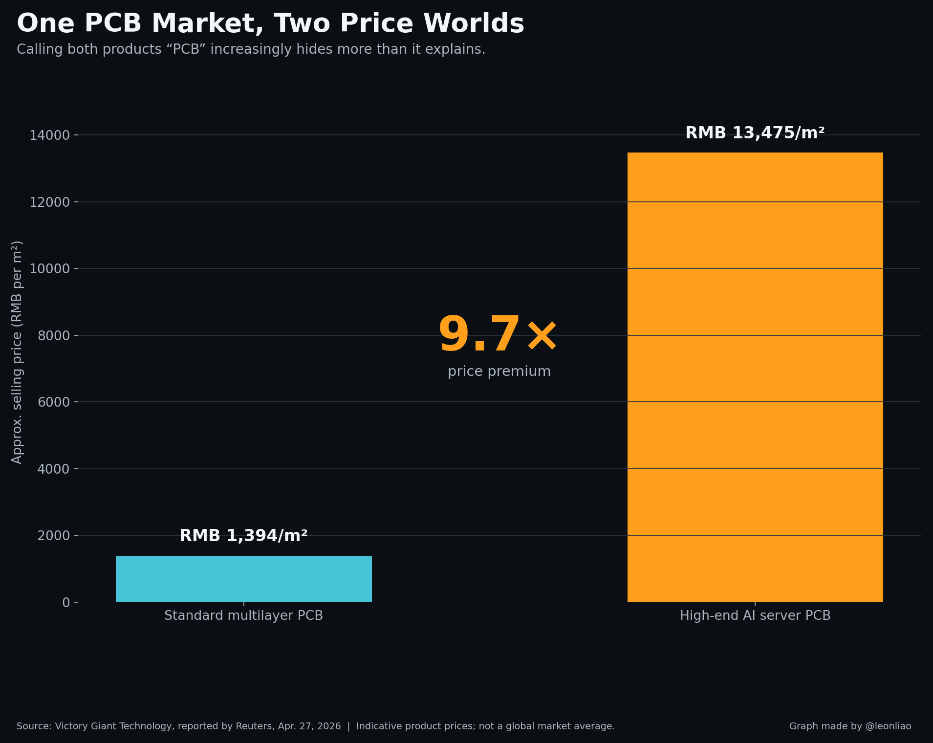
It is becoming difficult to treat this as mere product upgrading within a single PCB market. The large volumes of conventional FR-4 boards used in consumer electronics remain mature industrial products. They are highly price-sensitive, and their supply-demand cycles still move with smartphones, PCs and appliances. At the other end of the market, however, a different business is taking shape: high-layer-count, HDI, low-loss, high-speed and high-reliability PCBs for AI servers. Customers care more about delivery schedules, signal integrity, long-term reliability and supply continuity. A few hundred or even a few thousand dollars of additional PCB cost matters far less than a delayed GPU deployment.
The split is visible in margins as well as prices. Victory Giant reported a 43.5% gross margin for HDI in 2025, compared with 24.4% for multilayer PCB and 19.9% for basic single- and double-sided boards. JPMorgan expects the divergence to widen further by 2027: 46.7% for HDI and 35.2% for MLPCB, while conventional single- and double-sided boards remain almost unchanged at 20.1%.
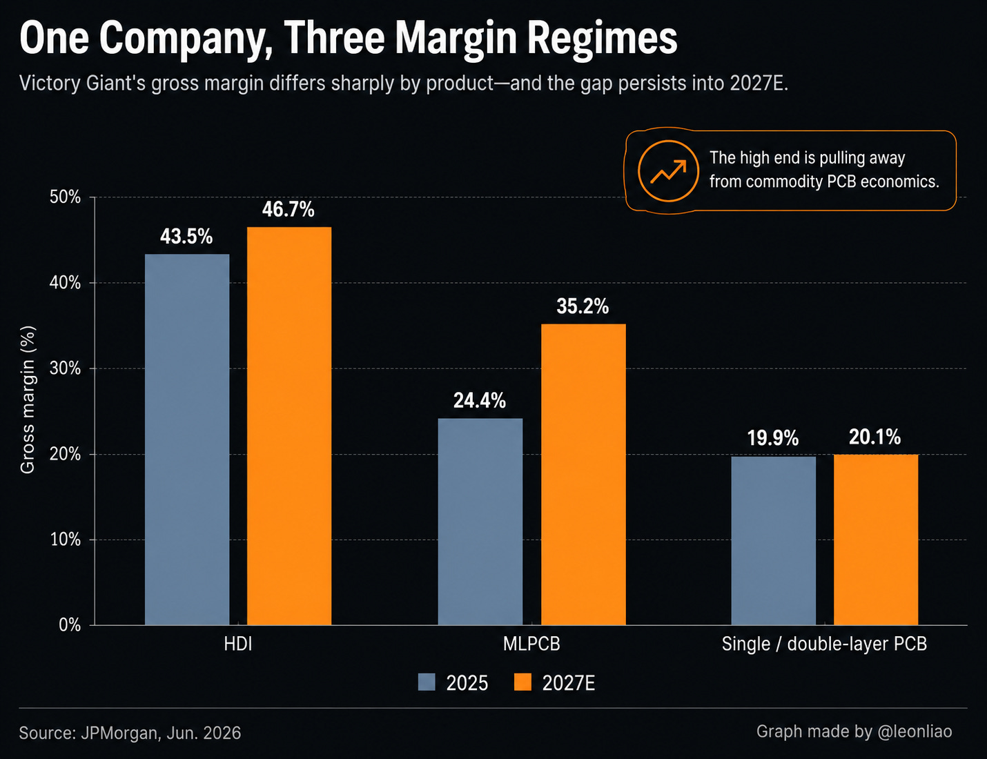
The high end is no longer behaving like a commodity PCB business. The same company, using the same broad manufacturing base, is effectively operating three different margin regimes depending on how far up the technology stack the product sits.
AI Is Redefining What a PCB Is Worth
At first, the story looked simple: AI servers needed more boards. Even in the A100 era, industry estimates suggested that the PCB content of an AI server was already several times that of a conventional server, with much of the incremental value coming from GPU-related boards. AI servers were beginning to detach PCB value content from the economics of traditional CPU servers. Blackwell has pushed that shift from the server level to the rack level.
A GB200 NVL72 rack contains 72 Blackwell GPUs and 36 Grace CPUs. The system is built around 18 compute trays and nine NVLink switch trays, with thousands of copper connections linking GPUs into a single scale-up domain. Fifth-generation NVLink raises bidirectional bandwidth to 1.8TB/s per GPU. At this point the PCB is doing much more than holding components together. It must carry larger currents, faster signals, denser routing and much tighter impedance and timing tolerances. Every jump in GPU performance forces the board to rebalance physical size, layer count and allowable signal loss.
Rubin raises the pressure again. NVIDIA’s Vera Rubin systems double per-GPU NVLink bandwidth to 3.6TB/s. Faster chips do not make signals travel across a board automatically. As frequency rises, skin effects intensify; microscopic copper roughness creates additional conductor loss; the dielectric constant and dissipation factor of the resin begin to affect signal integrity; even the weave of the glass cloth can introduce skew. Material differences that barely mattered in ordinary consumer electronics become system-level performance variables at hundreds of gigabits per second and beyond.
The whole PCB stack has had to move upmarket at once. Layer counts rise. HDI content increases. Laminate systems move from M7 toward M8 and M9. Copper foil progresses from VLP and HVLP toward ever lower surface roughness. Conventional E-glass begins to give way to low-Dk, low-CTE and increasingly specialized glass systems. One industry study, for example, traces compute-tray HDI from roughly 16–18 layers in H100 to about 20 layers in GB200, 22 in GB300 and 26 in Rubin, while high-layer interconnect boards move upward at the same time; it also maps the material transition from M6/M7 toward M8 and eventually M8.5/M9, with copper foil moving from HVLP2 toward HVLP4. These remain industry estimates rather than NVIDIA specifications, but the direction is consistent across the supply chain.
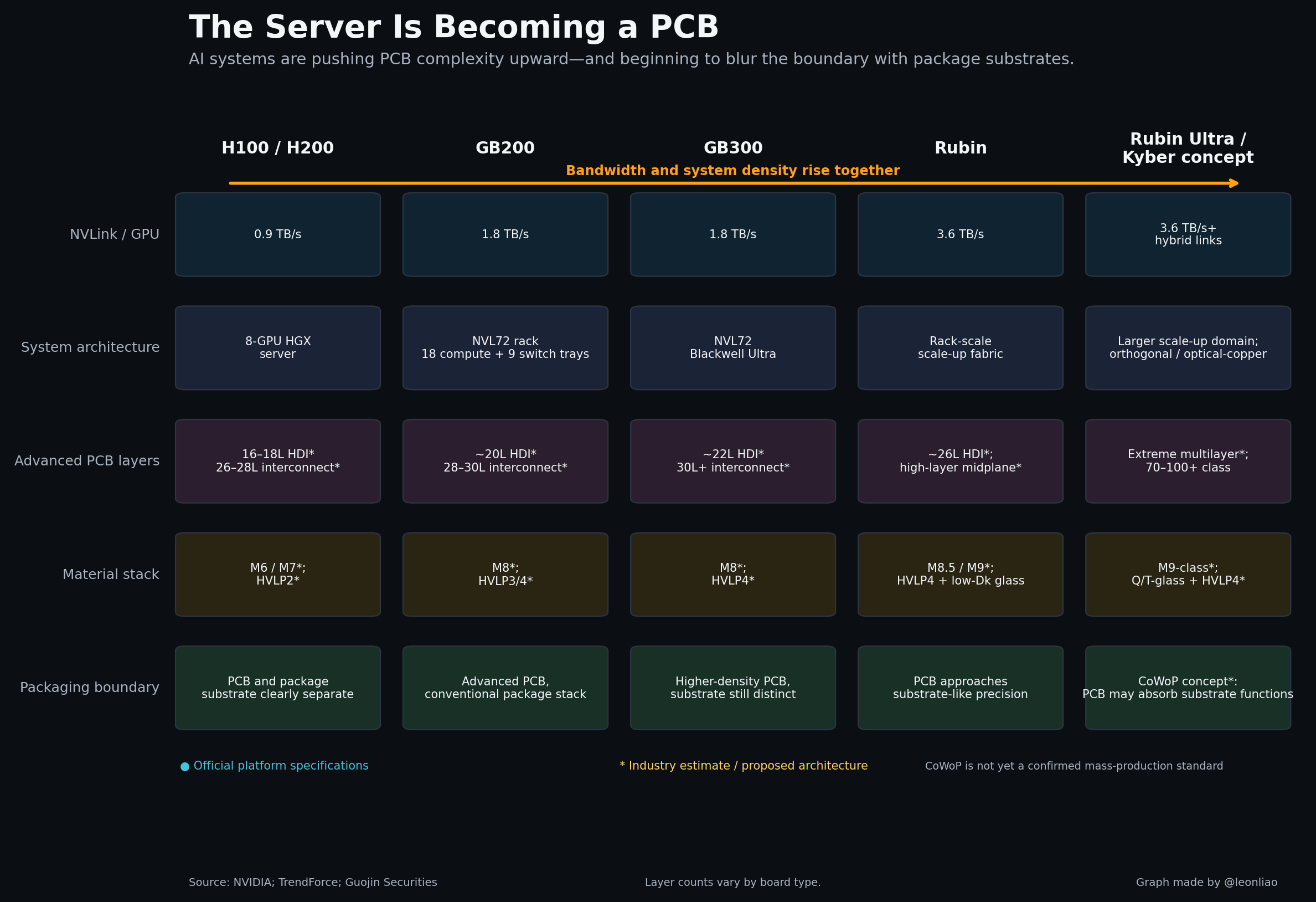
More GPUs explain only part of the increase in PCB value. The bigger change is architectural. In the Hopper era, the PCB primarily carried the computer. By the Rubin era, the PCB is increasingly becoming part of the computer’s interconnect architecture.
And one proposed next step goes further still.
The Boundary Between PCB and Package Substrate Is Beginning to Blur
For decades, the boundary was conceptually clean. The package substrate handled the dense interconnect immediately beneath the chip; the PCB connected packaged devices to the rest of the system. CoWoP—still an emerging architecture rather than a mature production standard—suggests that this boundary may become less rigid.
One proposed CoWoP configuration removes the conventional package substrate and connects the interposer more directly to the PCB. The attraction is obvious: shorter electrical paths can improve signal integrity; voltage regulation can be brought closer to the GPU; thermal design can be simplified; and removing part of the traditional package stack can reduce warpage and parasitic resistance. Industry research has described NVIDIA as studying such a route for future AI systems, but it should still be treated as a technology direction under evaluation rather than a confirmed mass-production architecture.
The significance lies less in whether one exact CoWoP implementation wins. The important point is that PCB manufacturing is beginning to acquire some of the process disciplines and economics once associated mainly with package substrates. Fine-line patterning, mSAP, laser direct imaging, tighter dimensional control and semiconductor-style customer qualification are entering parts of the AI PCB stack. AI PCB seemes to be retaining the large-format, multilayer-lamination foundation of traditional PCB manufacturing while moving toward package-substrate-like precision in materials, interconnect density and signal integrity.
That makes “PCB semiconductorization” a useful shorthand, but only if used carefully. The industry is not abandoning PCB manufacturing for semiconductor fabrication. It is importing more of the precision, capital intensity, qualification discipline and yield sensitivity of the semiconductor world.
Layer Count Is Only the Beginning
PCB manufacturers like to describe product difficulty in terms of layer count because it is easy to understand. It is also easy to misread. A factory capable of producing a 40-layer PCB cannot necessarily manufacture a 40-layer AI-server board reliably. Producing a 100-layer sample does not mean the supplier has commercial 100-layer capacity. Commercial capacity exists only when the materials, equipment, process control, board size, yield and customer qualification all work at the same time.
High-speed digital signals travel through PCB structures formed jointly by copper conductors and dielectric materials. As SerDes speeds rise, every increment of dielectric and conductor loss eats into the signal budget. Conventional FR-4 remains perfectly adequate for most consumer electronics. But in AI switches, GPU interconnects and high-speed networking boards, Dk, Df, thermal expansion and copper surface roughness become part of system design.
Manufacturing complexity rises at the same time. More layers mean more lamination cycles, each adding risks of registration error, warpage, resin-flow variation and drilling inaccuracy. HDI introduces laser microvias, stacked vias and more demanding electroplating processes. Larger boards compound the problem. AI systems are not becoming physically smaller: large compute trays and switch boards demand far greater dimensional uniformity than smartphone PCBs, and small thermal-expansion errors become much more consequential across a large panel.
Yield determines how much nameplate capacity turns into usable output. A 100-layer board may command a premium, but if yields are half those of a conventional board, much of the factory’s nameplate capacity is illusory. Victory Giant already has mass-production capability in 70-layer-plus multilayer PCB and is investing further in 24–36-layer HDI, yet JPMorgan still builds potential margin pressure from yield and utilization ramp into its forecasts.
Even the drill bit becomes part of the story. Thicker boards, smaller vias and harder high-end materials increase consumption of high-aspect-ratio, coated and ultra-small micro-drills. One industry study puts the global PCB drill-bit CR4 at 70.5% and notes that more demanding M9-class materials accelerate tool wear. A previously mundane consumable becomes another high-end bottleneck as board complexity rises.
AI PCBs are therefore changing what the industry means by “capacity.” In the past, it was enough to ask how many square meters of PCB a factory could produce each year. Today, the more relevant question is: how many square meters can be built with advanced low-loss laminates, HVLP copper foil and high-performance glass, using the right equipment, at an acceptable yield, and then pass NVIDIA or hyperscaler qualification?
The world does not lack PCB factories. It lacks that kind of capacity.
The Fastest-Growing Products Are the Hardest to Expand
The overall PCB industry is still growing, but AI-related products are pulling away from the market average. According to Prismark-related forecasts, the global PCB market is expected to grow at roughly 8% annually over the next several years. AI-server PCBs are expected to grow much faster, with HDI and high-layer-count products growing faster still.
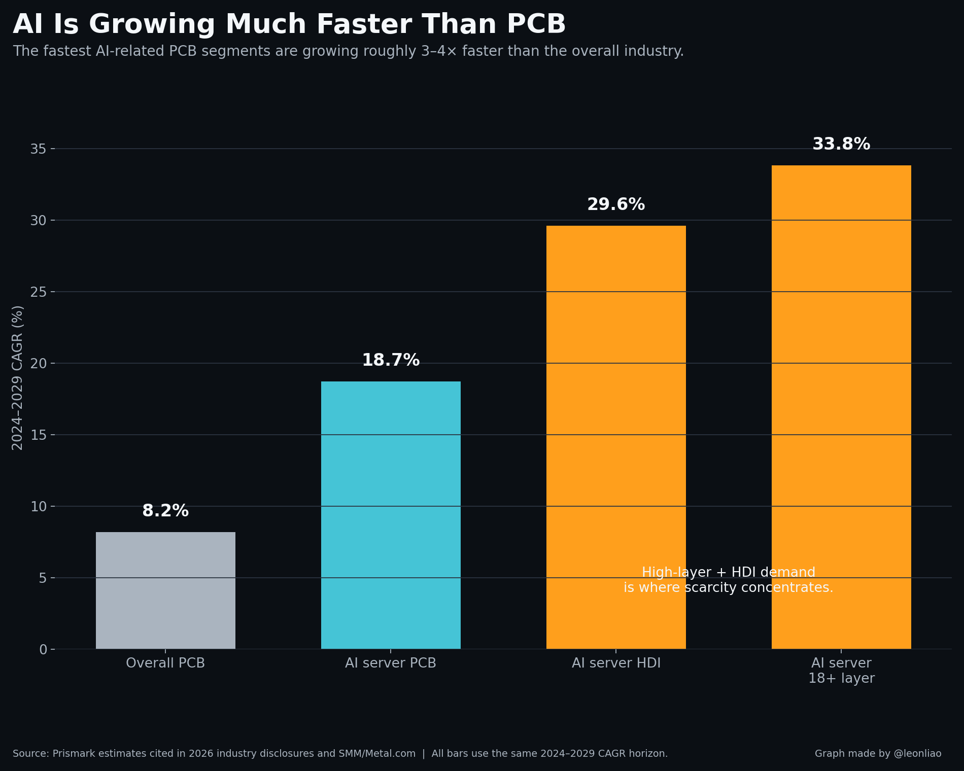
That growth pattern almost guarantees bottlenecks. The easiest products to expand are growing the slowest, while the most technically demanding products are growing the fastest. When conventional PCB prices rise, manufacturers can increase utilization, extend operating hours or shift some capacity from adjacent products. High-end AI PCBs are harder to substitute. Their materials, equipment configurations, process parameters and customer certifications differ. Building a new production line is only the beginning; process tuning, sampling, qualification, yield ramp and mass-production reliability testing all come afterward. Effective capacity can emerge several quarters after a factory is physically completed.
WUS Printed Circuit has already shown what this product shift looks like in practice. Much of its recent growth came from AI servers, high-performance computing and high-speed switching, with demand for high-speed switches and routers particularly strong. Higher-end capacity has increasingly been allocated to core products for leading customers. Shengyi Technology has seen the same process from the CCL side: years of qualification and customer development are turning into real AI orders, while rising prices for glass cloth and copper foil are prompting earlier procurement and repricing across the supply chain.
NVIDIA is only one part of the demand story. North American cloud providers are accelerating their own ASIC programs, creating a second engine for high-end PCB demand. One brokerage estimate puts ASIC AI-server share at 27.8% in 2026, while pointing to Google, Amazon and other CSP platforms as additional sources of demand for high-layer-count and highly customized boards. JPMorgan makes the same point at the company level, arguing that Victory Giant’s exposure to Google and other ASIC projects could add to the gains from NVIDIA’s Blackwell-to-Rubin transition.
AI is doing two things at once: increasing the number of boards required and pushing demand toward the hardest boards to manufacture. Quantity and product sophistication are rising together, and supply cannot respond simply by running existing factories harder.
The Bottleneck Is Moving Upstream—and Into the Equipment Itself
Looking only at PCB manufacturers produces an obvious conclusion: Victory Giant, WUS, Gold Circuit Electronics and other high-end board makers need more capacity. Move upstream, however, and the supply base gets narrower.
PCBs require copper-clad laminate. CCL in turn requires resins, glass cloth and copper foil. Every performance requirement imposed by an AI server is transmitted into these materials. Lower signal loss requires better resin systems. Greater dimensional stability requires lower-CTE glass. Faster signals require smoother copper foil.